What We’ve Been Up To:
Heavy Copper
Aurora Circuits has developed a unique process to maximize the thermal conductivity of PCB pads. We hosted a webinar on this very topic, and, for all of the engineers/PCB designers, please see a few details below:
Design Concept:
High Power applications – Power, Lighting, High Current – High Watt LED arrays, Power Transistors, Amplifiers, etc. What components are to be used and what level of heat generation needs to be dissipated. What methods of heat removal can be utilized to dissipate heat from the system – Conduction, Convection or Radiation?
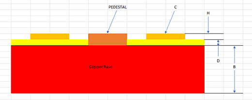
The design based on components with thermal pad on bottom for direct attachment (soldered) to a Pedestal Pad:
For a direct thermal path of a copper connection to a copper base plate for best connection to a heat sink . Allows maximum thermal conductivity at 380W/mK as compared to Thermal Dielectrics that are typically rated from 1 to 10W/mK*. Benefits of Pedestal Pad construction: Top of Pedestal is at same height (planarity) with all other circuitry pads Pedestal structure is Electroplated Copper for durability and compliance Surface finish the same as circuitry pads. Processed cost is comparable to top rated IMS materials with much better (10X+) performance. Most rapid heat removal to minimize heat rise leads to longer component life, performance, reliability and safety

C = Circuit Copper – typical foil thickness is 1oz or 2oz – Can be other.
D = Dielectric Thickness – thin dielectrics used are 25-75µm/.001-.003”.
H = Pedestal Height = Dielectric + Circuit Thickness – Created by Copper Plating so thicker Dielectrics or Circuit Copper will require thicker plating.
B = Copper Base Plate – Thickness typically 1.5mm/0.059” or 1.0mm/.039”
Rigidity needed for flatness and attachment to external Heat Sink.
US Electronics Spotlight
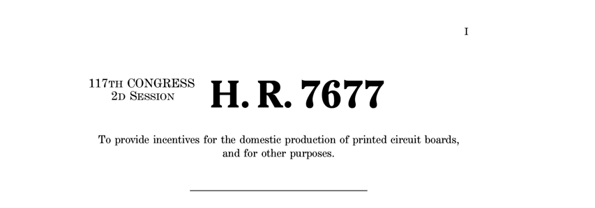
Supporting American Printed Circuit Boards Act of 2022: An Appraisal
We recently released a blog post that broke down the recent PCB bill proposed in Congress. While it could be a boon to our industry, further examination and input is (we feel) necessary to appropriate the funding for maximum industry return. The domestic PCB industry and US government has one shot to get this right–the stakes cannot be higher; therefore, US PCB industry leaders must be able to make recommendations to this proposal, ensuring taxpayer funding is sensibly distributed.

A lot has changed over the past 80 years, but what hasn’t changed is Aurora Circuits dedication to remaining 100% American Made. With over 80 years of knowledge and experience to make your project a reality, we stand by our commitment to manufacture the highest quality products founded on expertise and innovation.


