What We’ve Been Up To:
Heavy Metal
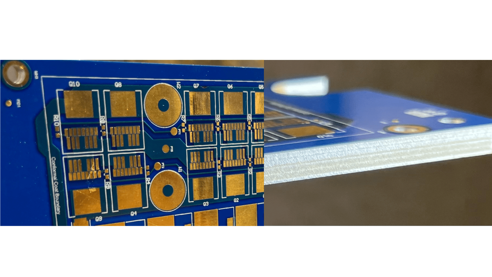
Aurora Circuits oftentimes comes across as a “machine shop” due to our work with heavy copper, IMS substrates and countersinking capabilities. While we make PCBs, the need for increased thermal conductivity has pushed us into this metal working arena at an ever increasing pace. The aluminum substrate on this board (images below) is “0.190/4.82mm thick-quite a feat drilling and routing this complex design, as it’s not a single sided board. This is actually a two layer PCB laminated to the substrate. We continue to push the boundaries of MCPCBs-please let us know if we can assist you in your next “heavy metal” project.

Blog Preview
The Designer’s Guide to Heavy Copper Printed Circuit Boards
This excerpt is from our newest blog on heavy copper. We wanted to share more details regarding the application, process steps and unique characteristics of heavy copper PCBs. Please feel free to access the entire post here.
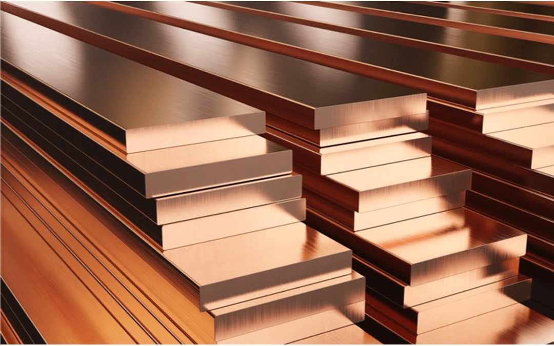
Most commercially available printed circuit boards are manufactured for low-voltage/low power applications, using copper traces & planes made up of copper weights ranging from 1/4 oz/ft2 to 3 oz/ft2 on both inner layers and the outer layer finished surface. Heavy copper is then generally defined as anything greater than 3 oz, with some power designs routinely calling for 15 – 20 oz of solid copper. Copper weights above 20 oz/ft2 and up to 200 oz/ft2 are also possible and are often referred to as Extreme Copper. Thermal management is more important than ever in today’s new designs as electronics are used in demanding environments and operate at higher currents. Heavy copper PCBs can help conduct heat away from components so failure is greatly reduced. These heavy copper PCBs conduct electricity better and are more capable of withstanding the increased thermal stress while under power.
Top 10 Applications of Heavy Copper PCBs
Power Supplies/Converters
Automotive
Electric vehicle charging stations
Power Distribution
Solar Panels
Power line monitors
Weapons & radar control systems
Traction converters for rail applications
Power grid switching systems & backup
Renewable energies and storage pumping plants
Overload & protection relays

A lot has changed over the past 80 years, but what hasn’t changed is Aurora Circuits dedication to remaining 100% American Made. With over 80 years of knowledge and experience to make your project a reality, we stand by our commitment to manufacture the highest quality products founded on expertise and innovation.


