


Parasitics in electronics are a persistent and often underestimated challenge that engineers and designers encounter in the development of electronic circuits and systems. Parasitic elements, which include stray capacitance, inductance, and resistance, can have a significant impact on the performance and functionality of electronic devices. Understanding and mitigating these parasitics is crucial for achieving the desired performance and reliability in electronic systems.
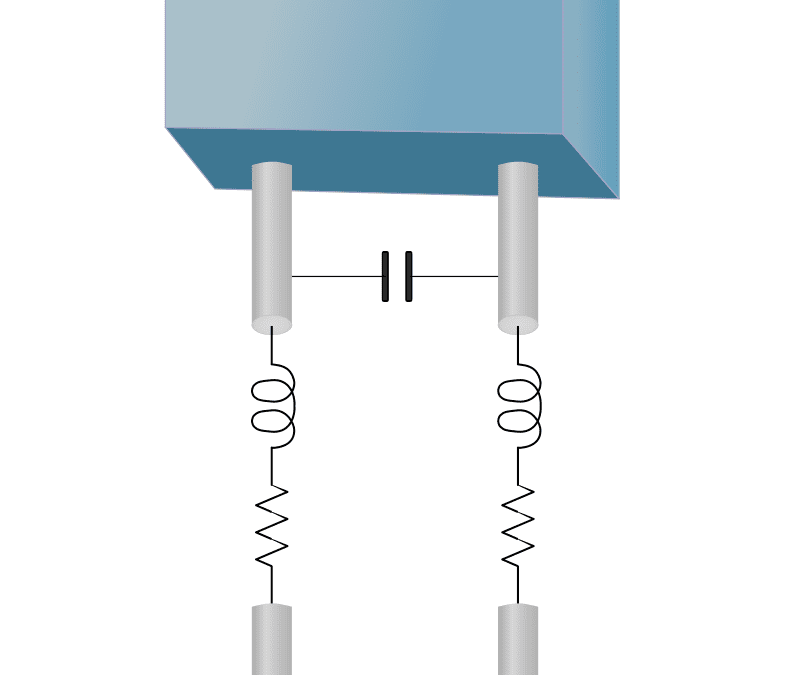
Stray capacitance is one of the most common parasitic elements in electronics. It occurs when two conductive elements are separated by an insulating material, such as the dielectric in a printed circuit board (PCB). Stray capacitance can lead to unintended coupling between various parts of a circuit, affecting signal integrity, impedance matching, and circuit response. For high-frequency and high-speed applications, stray capacitance can result in signal distortion and cross-talk between adjacent traces, leading to data errors or interference.
Stray inductance is another significant parasitic element in electronic circuits. It arises from the conductive paths formed by traces, wires, or components and can have a detrimental impact on circuits, especially in high-frequency and high-current applications. Stray inductance can result in voltage spikes, ringing, and electromagnetic interference (EMI). These effects can damage components and disrupt the normal operation of a circuit. Managing stray inductance is crucial to ensuring circuit stability and preventing unintended consequences.
Parasitic resistance is yet another challenge in electronics, although it is often less pronounced than capacitance and inductance. Parasitic resistance can lead to power losses, voltage drops, and increased heat generation in electronic components. In power electronics, where efficiency is critical, even small parasitic resistances can have a substantial impact on the overall performance of a system. Careful consideration of parasitic resistance is essential to minimize power losses and maximize system efficiency.
Mitigating the challenges posed by parasitic elements in electronics is a complex task that requires careful design, analysis, and testing. There are several techniques and strategies that engineers use to address parasitics:
- Component Placement and Routing: The physical layout of components and traces on a PCB can affect parasitic elements. Careful placement and routing can minimize stray capacitance and inductance. Techniques like differential routing and guard traces can help manage parasitics effectively.
- Grounding and Shielding: Proper grounding and shielding techniques can reduce the impact of parasitic elements on circuit performance. Ground planes and shields can help minimize electromagnetic interference and reduce parasitic capacitance and inductance.
- Component Selection: Choosing components with low parasitic elements is crucial, especially in critical applications. Components with low ESR (Equivalent Series Resistance) and ESL (Equivalent Series Inductance) are preferred to minimize parasitics.
- Impedance Matching: Impedance matching techniques can help reduce the impact of parasitic capacitance and inductance, especially in high-frequency applications. Techniques like controlled impedance PCB design are essential for maintaining signal integrity.
- Simulation and Modeling: Advanced simulation tools and modeling software can help engineers analyze and predict the effects of parasitic elements on a circuit. This allows for early identification and mitigation of potential issues.
- Testing and Validation: Rigorous testing and validation are essential to ensure that parasitic elements do not adversely affect the performance of electronic systems. High-frequency testing, time-domain reflectometry, and network analyzers are commonly used tools for this purpose.
Parasitic elements in electronics present significant challenges to engineers and designers. These unintended capacitance, inductance, and resistance can affect circuit performance, signal integrity, and overall functionality. To address these challenges, engineers must employ a combination of design techniques, component selection, simulation, and testing. Minimizing the impact of parasitics is crucial to ensuring the reliability and performance of electronic circuits and systems, particularly in high-frequency, high-speed, and power-sensitive applications.